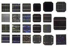
Company Profile:

Evonik Industries is one the world’s lead specialty chemical companies. One of the main goals of the company is to provide product that solve problems and provide a maximum benefit to customers and society. Recently, they have developed a more fuel efficient tire that does not compromise on performance through the implementation of a silica-silane system, known as ULTRASIL.
ULTRASIL:
The greenhouse effect is a natural process in which radiant heat from the sun is captured in the lower half of the atmosphere, directly resulting in higher temperatures and thus global warming. In order to reduce this greenhouse effect, most companies are working towards minimizing carbon dioxide emissions from transportation. Carbon emissions from combustion of energy fuels has accounted for 81.5% of total greenhouse gas emissions over the last several years, and global warming is quickly becoming a major problem throughout the world. Transportation contributes to this on a large scale, and it is responsible for 31% of the CO2 emissions from the United States. However, Evonik’s silica-silane system (ULTRASIL) is a unique approach to this problem. ULTRASIL is created in several different forms and is applicable in many different situations, however its primary purpose is to serve as a coating for tires. This advanced tire technology can reduce the rolling resistance of tires, increase traction in wet conditions, and reduce carbon dioxide emissions. In general, tires have been targeted as quick way to reduce carbon dioxide emissions, as simple changes in size and shape can increase fuel efficiency by up to 15%.

ULTRASIL is able to reduce rolling resistance between tires and wet or icy road conditions due to the presence of intermolecular forces (IMFs), which can determine whether a solid will be hydrophobic (resists water) or hydrophilic (attracts water). This is an important concept to the concept of ULTRASIL because it is produced with hydrophobicity in mind. Being hydrophobic, water will adhere to the ULTRASIL coated tires, resulting in increased traction between the tires and the road. The major types of intermolecular forces that impact hydrophobicity include dipole-dipole forces, hydrogen bonding, ionic interactions, and London dispersion forces.
Dipole-dipole forces, hydrogen bonding, and ionic interactions are all known to be hydrophilic interactions. The larger presence of these forces in a molecule, the more the solid will attract water molecules. Dipole moments in a molecule are dictated by the polarity of a molecule. Polarity is the sum of all of the bond polarities in a molecule, resulting in dipole moments. The dipole moment is measured in a vector as the sum of the individual vector movements. For example, CO2, a linear and non-polar molecule, has no dipole moment. Hydrogen bonds are the interactions of a hydrogen atom with a nitrogen, oxygen, or fluorine atom. They are a much more powerful force than dipole-dipole forces, resulting in a larger increase on the hydrophilicity of the molecule. Similarly, the presence of ionic bonds (interactions between positive and negative ions) can have the same effect.
London dispersion forces, the weakest of the intermolecular forces, are the sole forces that can raise the hydrophobicity of a molecule. This force, also called an induced dipole-dipole force, is a temporary attractive force that results when the electrons in two adjacent positions occupy positions that make the atoms form temporary dipoles. These forces occur in all molecules. In the production of ULTRASIL, Evonik has created a silica-silane system, where the hydrophobic regions of the molecule dominate, causing adhesive forces to arise and increase the tension between tires and wet/icy road conditions. More information about intermolecular forces can be found here, or
Also, the chemical structures of the silica helps contribute to its unique properties. Silicon dioxide can exhibit one of the largest varieties of crystal structures among the compounds commonly available and used. These many different crystalline forms allow silica to be used in a broad range of applications, including ULTRASIL. Precipitated silica, which is key to this product’s functionality, is a specially prepared form that has an amorphous structure, similar to silica gel or glass, both of which are predominantly silicon dioxide, or silica. As already discussed, adding these silicon dioxide granules to the surface of rubber tires has many beneficial effects on vehicle performance, but binding this hydrophilic molecular solid to the long, continuous, and hydrophobic polymer chains that make up vulcanized rubber can be difficult. It is up to sulfur, linking the polymers of vulcanized rubber to make it more resistant to temperature extremes, to act as a coupling agent for silica, since the hydrocarbon polymers will not bond to it by themselves.

From what we know, however, ULTRASIL production takes a rather different approach to solving the problem of coupling silica to rubber: the silica-silane system. By treating the original rubber material with various organosilanes, a surface that silica particles can easily bond to is created, making it possible to form the desired composite with more cross-links to the silica granules and a higher overall thermal stability than without the treatment. Organosilanes usually have both a nonpolar and polar end and can not only bond with vulcanized rubber, but also with the silicon dioxide particles, through dehydration synthesis of their hydroxyl groups with the hydroxyl groups that cover the surface of the silica particles.

While many of the specific details of the ULTRASIL manufacturing process are trade secrets of Evonik, the company does share the basic concept of how it obtains the very pure amorphous silica needed for its products: precipitation from solution. Precipitated silica is widely used in industrial processes around the world, and Evonik Industries is its largest producer. Just like in ULTRASIL, these fine silica grains are often used in rubber products like tires and shoe soles for benefits similar to those of Evonik’s products. Generally, an aqueous silicate salt is reacted with an inorganic acid (like H2SO4) to form insoluble silica in the following reaction:
Na2SiO3(aq) + H2SO4(aq) → SiO2(s) + Na2SO4(aq) + H2O(l)
After the silica precipitate has been dried, it still contains no more than 88% silicon dioxide according to Evonik, with most of the rest being water. The ensuing treatment to purify the product varies depending on the desired size and quality of the particles obtained, but eventually a fine powder consisting of 99% silica can be obtained. The precipitated silica used in the ULTRASIL product line consists of miniscule, porous granules often of nanoparticle size to allow a high surface area to volume ratio, with the 7000 GR variant having a surface area of 170 m2 per gram. It is this kind of fine silica that allows for the reinforced rubber of the emerging “Green Tire” that advances in silica rubber have created.
Further Reading:
If you are interested in the chemistry behind Evonik’s ULTASIL, there is a lot of in depth reading available in scientific journals. A thorough account of this technology and the chemistry that drives it can be found


 Graphic credit to Marc Marshall, Schatz Energy Research Center/

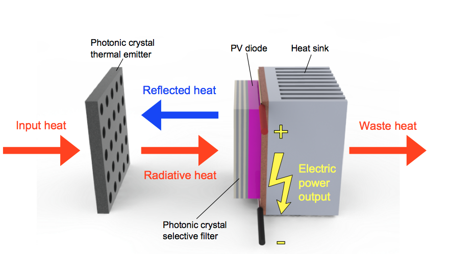

 Due to the holes that are formed within the semiconductors, they are ideal to use within photovoltaic cells. “Why?” you may ask. In order to induce an electric field inside a photovoltaic cell, two semiconductors are put together, one P-type semiconductor and one N-type semiconductor. The P and N correspond to positive and negative respectively. In a P-type semiconductor, there is an abundance of holes while an N-type semiconductor has an excess of electrons. By putting a P and N-type semiconductor together, a P-N junction is formed where they meet.


